Some of you may recall my complaining about the lack of USB oscilloscopes for the Mac a couple of years ago, when I bought myself a used Kikusui COS5060 analog oscilloscope. In the comments for my complaint post, someone named Chris had recommended last March that I check out bitscope.com, as they supposedly had software for the Mac OS X.
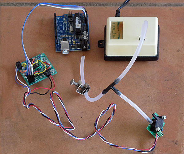
This year for my birthday, I bought myself the Bitscope Pocket Analyzer, a tiny (6.6 × 6.2 × 1.7 cm) USB attachment that can act as a 2-channel oscilloscope, plus a few digital channels, plus a waveform generator. The price is a little high (about $300) and it was a hassle to buy, because my credit card company was convinced that a transaction from Australia had to be fraudulent, and didn’t get around to checking with me for a couple of days, after rejecting the purchase three times. Luckily the bitscope people were very nice about it and even gave me free faster shipping, which was very generous, as none of the delays had anything to do with them—just with my miserable excuse for a bank (I’m looking at you, Wells Fargo!).
The bitscope does have software for the Mac OS X, which is appropriately labeled as beta-release software. There are still bugs in it (for example, when I try to save a screen shot in jpg format, it saves it in png format instead), but most of the functionality one would want is there. Saving also only saves the main scope display, not all the setting displays around it (so there is no record made of most of the settings, and any cursor readings have to be manually recorded, or you use the screen-shot features of your operating system). The value displayed on the screenshot that is saved is the “bias” or mean waveform voltage—perhaps the most useless of the measurements they could have chosen to make the displayed one. There are probably other bugs, but I’m still unfamiliar enough with the controls that I usually can’t tell when I’m making a mistake vs. when the software is.
Like other digital scopes, the Bitscope records a full frame before displaying anything, and it alternates a frame of channel A with a frame of channel B. This can be rather disconcerting if you are using a slow time base (like for an EKG signal), as nothing appears on the screen for a few seconds after the trigger. With higher speed time bases, the frame rate is fast enough that the delay is not noticeable.
Also like other digital scopes, the controls are highly idiosyncratic and difficult to learn. In the case of the bitscope software, the controls are even more idiosyncratic than usual—they have something they call “Act on Touch” controls, which behave differently depending where on the button you click:
click and drag up and down or left and right on a parameter to adjust its value. Click on the left or right edge of the parameter to select a previous or next value.
Right-click (or control-click on a Mac or press-and-hold on a tablet) to pop up a context menu and double-click to open an editor to type in a value or select a default value.
Note that the cursors cannot be adjusted by this “Act on Touch” method nor with the arrow keys, but can only be dragged on the image, which makes measuring some parameters more difficult that in needs to be.
I did eventually manage to do some plots that correspond to the taking the thresholds of a pMOS field-effect transistor (pFET) and an nMOS field-effect transistor (nFET).

Test circuits for determining thresholds of the FET transistors. I only hooked up one of the test circuits at a time (nFET or pFET), not both at once.

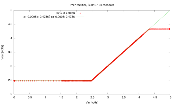
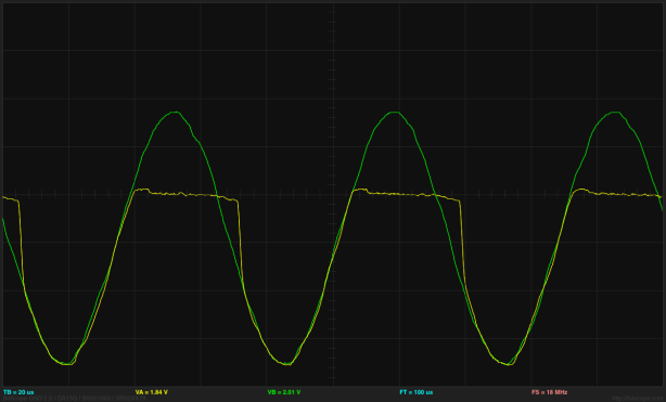
Results for testing the NTD2955 pMOS FET. I set the cursor about where the transistor turns on, at 2.08V, which gives a threshold voltage of 2.08V-4.93V= -2.85V, close to the nominal -2.80V, and well within the specs (-2.0V to -4.0V).
I see that I ended up with non-standard vertical scaling here for channel A (the Vp voltage). Changing the range of the inputs picks non-standard scaling by default (another stupid choice by the software designers).
The curve clearly shows the quadratic dependency of the current on the gate voltage above threshold. With a little more care in using the bitscope, I can see that I get 1v (100mA) when the voltage is 1.56v (so -3.37 relative to the source), which would give me something like I= 370(2.85V+VDS)2 mA/V2.
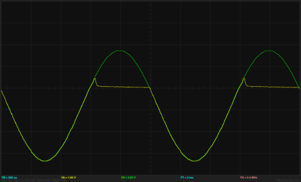
I also did a similar plot for an nMOS FET:

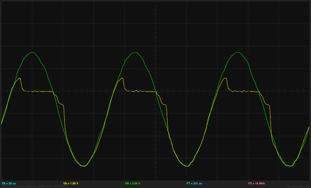
Bogus threshold plot for NTD5867 nMOS FET. The current does not seem to follow a quadratic curve above the threshold voltage, because the 5.2V range on Channel A is truncating part of the curve (which goes from -2.6V to +2.6V, not 0V to 5.2V).
The current for the nFET peaked at almost 500mA, which is a 2.5W power dissipation: far more than the lowly ¼W resistor could handle even for a short duty cycle. I had to pull the power wire from the breadboard quickly after each test, to keep from burning up the resistor. I did not repeat this test with a 10Ω resistor, but switched to a 100Ω resistor for safety. If I have the students measure the thresholds for their FETs, I’ll have to make sure they compute the minimum resistance value that they can safely use with the voltage they are testing at, and not just blindly grab a convenient size that was sitting around on the benchtop, as I did.

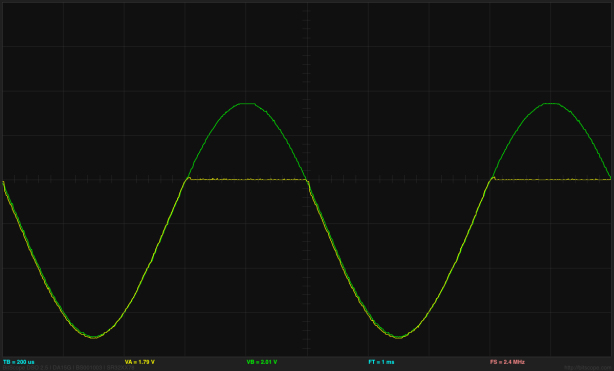
With a 100Ω series resistor, I detect the nFET turning on at 1.66V, and see the expected quadratic dependence of the saturation current on gate voltage above threshold. The 1.66V is not close to the nominal 1.8V threshold, but is within specs (between 1.5V and 2.5V).
The 100Ω resistor does not get warm, as the 0.25W max power dissipation times the approximately 1/3 duty cycle is well within the ¼W power limit. Using a larger resistor makes the threshold detection a little easier, since turning the transistor on only a little to get 1mA of current, provides an easily seen 0.1v swing.
At a gate voltage of 2.08V (0.42V above threshold), the output current is 40mA, so the saturation current is about 227(VDS-1.66V)2 mA/V2.
Now that I’ve characterized the FETs, I should probably try designing a power amp using them. I tried several designs this morning in CircuitLab, but the circuit lab simulator has serious problems with op amp circuits. It gets confused by the feedback loops and neglects to bound the voltage values, so I was getting DC “solutions” with outputs in the teravolts. It would be quite a trick to get a teravolt output from an op amp with a 5v power supply!
Some of my designs were quite clever—one that I was curious about used DC coupling throughout, but automatically compensated for the DC offset of the microphone and should keep the voltage across the speaker centered without needing a dual-rail supply (that is, no high-current center supply) nor large DC-blocking capacitors. It took 4 op amps and a differential amp, though, so was not a cheap solution (if it even works—I’ll have to wire it up to find out, as the simulator couldn’t handle it).
I think I’d better try a couple of straight-forward designs and see how they work, first—designs the students are more likely to come up with.
Filed under: Circuits course, Uncategorized Tagged: BitScope, circuits, FET, nMOS FET, oscilloscope, pMOS FET, threshold voltage, USB oscilloscope


 ). However, I am also constrained by the resistance of the inductor, since the sum of the resistance around the loop has to remain negative. Estimating the negative resistance by fitting a straight-line to the appropriate part of the V-vs-I curve gave me a negative resistance of –2.145Ω. So the inductor needs a DC resistance under 2Ω.


 = 2\cos^2(\theta)-1") , and reassured them that I did not expect them to remember trigonometry—this may be the only place this quarter where we use a trig identity.) I also had them derive the RMS voltage for a square wave, so they could see that the
, and reassured them that I did not expect them to remember trigonometry—this may be the only place this quarter where we use a trig identity.) I also had them derive the RMS voltage for a square wave, so they could see that the  ratio was a special case for sine waves and not a general phenomenon.
 formula. I suspect that most of them can handle the algebra for the exponential decay towards 0V, but that they will have trouble with expressing the exponential decay towards 4V (the output high voltage).

T_{10}") and
and T_{100}") . From these equations I got estimates of 78.5Ω and 0.410H. Note that the resistance includes all the wiring resistance, which was substantial, as I was using flexible jumper wires that are not made from copper and have a high resistance.
. From these equations I got estimates of 78.5Ω and 0.410H. Note that the resistance includes all the wiring resistance, which was substantial, as I was using flexible jumper wires that are not made from copper and have a high resistance. . With this method, I measured the inductance and resistance as 0.369H and 73Ω. I also tested an AIUR-06-221 inductor (nominally 220µH and 0.252Ω) with a 1Ω current-measuring resistor and got 229µH and 0.258Ω.
^2 = 0.401 \mbox{H}") , or 0.418H, if we use 229µH as the inductance of the AIUR-06-221. Note that this measurement depends on knowing the inductance of the small inductor, but does not require knowing the capacitance of the ceramic capacitors—just that the capacitance is the same for either inductor.
, or 0.418H, if we use 229µH as the inductance of the AIUR-06-221. Note that this measurement depends on knowing the inductance of the small inductor, but does not require knowing the capacitance of the ceramic capacitors—just that the capacitance is the same for either inductor.


 , and the output voltage should be
 }{R_{2}}") for some constants A and B that depend on the transistor. Note that changing R2 just changes the offset of the output, not the scaling, so the range of the output is not adjustable without a subsequent amplifier.
for some constants A and B that depend on the transistor. Note that changing R2 just changes the offset of the output, not the scaling, so the range of the output is not adjustable without a subsequent amplifier.


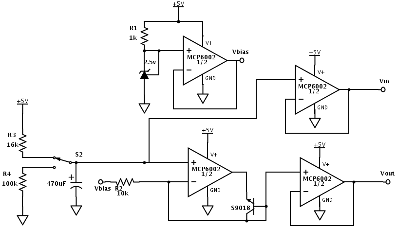
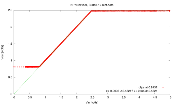
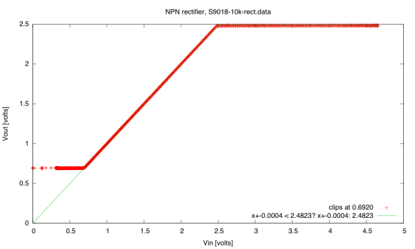
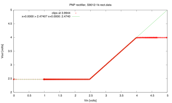


") . The output impedance is very low. Note that the difference in the output impedance for the two states is similar to the situation for the simpler circuit, and can cause problems if the output of the rectifier is fed directly to an RC filter, unless the R value for the RC filter is much larger than R2. For the loudness circuit, we want a very large RC time constant to smooth out the ripples of the rectifier, so a large R value is not a problem.
. The output impedance is very low. Note that the difference in the output impedance for the two states is similar to the situation for the simpler circuit, and can cause problems if the output of the rectifier is fed directly to an RC filter, unless the R value for the RC filter is much larger than R2. For the loudness circuit, we want a very large RC time constant to smooth out the ripples of the rectifier, so a large R value is not a problem.


 C_{1}") .
. and that
  (because β is large, so
  is a small fraction of the current). But
 R_{c}") . That means that the gain is
. That means that the gain is  . I said that this design was good for providing high voltage gain, but was not good for providing high current (because
  is large). I did not give them all the constraints on the components and signal levels needed to make sure that the amplifier works correctly.


